C0-microSD Design-in Guide
The C0-microSD drops into any host with a microSD slot that conforms to the 4-wire SD protocol or SD-over-SPI.
Typical application circuits
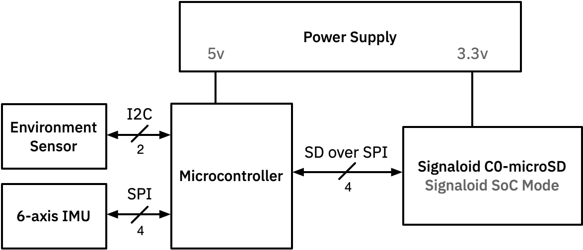 | 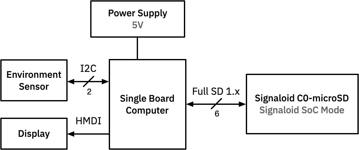 |
|---|
Example circuit of the Signaloid C0-microSD acting as a co-processor on a microcontroller-based embedded system (left), or on a single-board computer (right)
Power
Supply the module with 3.3 V on the microSD VDD pad (3.14 V to 3.5 V, see
Electrical characteristics).
The module generates its internal rails on-board, so the host only supplies VDD. Measured
current draw stays below 8 mA on the published reference workload, well within any standard
microSD slot budget.
Signal levels
The SD interface pads (pins 1 to 8) are LVCMOS 3.3. The SPI configuration port on the test pads (pins 9 to 14) is LVCMOS 1.8: connect external programmers at 1.8 V only. See Specifications → Pinout.
Socket or solder-in
The module works in a standard microSD socket (hot-swappable), or you can design it into a product using the standard microSD land pattern (see Specifications). For development, an open-top socket such as the one on the SD-Dev carrier exposes the test pads for probing.
Standalone FPGA integration
When the C0-microSD runs a custom user bitstream without an SD host, six microSD pads and five test pads become configurable I/O. Integration details for that use are in Modes and Custom Bitstream.
Next steps
- Pinout, the pin names, signal standards, and debug pads your design connects to.
- Compatibility, the SD host controllers and platforms already validated with the module.
- Handling and ESD precautions, the assembly, storage, and handling limits for the module.
- SD-Dev Carrier Board, a reference carrier for probing and power-cycling the module during bring-up.