C0-microSD+ Specifications
This page is the hardware reference for the C0-microSD+, whose full product name is the Signaloid C0-microSD+ Professional UxHw® Module. It collects the compute, memory, UxHw, electrical, thermal, and mechanical figures of the module in one place.
The module features the built-in Signaloid SoC, so a complete working session takes four steps. You flash your device application to the module, start the core, exchange data with the core over the SD interface, and stop the core.
The figures on this page come from C0-microSD+ datasheet revision 0.2, which is marked preliminary. Treat every figure as subject to change while the module is at the engineering-samples stage.
Compute and memory
| Component | Details |
|---|---|
| Signaloid C0 RISC-V-based SoC |
|
| FPGA | Lattice CrossLink-NX-33 (LIFCL-33-8USG84C), with
|
| Non-volatile memory | 128 Mb (16 MiB) SPI flash |
| GPIO | 9 GPIOs in total, comprising
|
The 320 KiB of on-chip memory that the Signaloid SoC uses as its main memory is the Large RAM (LRAM) of the FPGA.
UxHw capabilities
| Parameter | Value |
|---|---|
| Maximum representation precision | Athens-64 |
| Number of in-flight distributions | 4312 (Athens-8) 476 (Athens-64) |
| I/O minimum latency (read / write)* | 0.8 ms / 6.0 ms |
| I/O maximum throughput* | 100 Mbit/s |
*I/O latency and throughput are measured on transactions of 512-byte blocks using the
dd command.
Signaloid SoC Core details
| ISA | ABI | Operating frequency | Available memory |
|---|---|---|---|
| RV32IMFC | ilp32f | 90 MHz | 320 KiB |
The Signaloid SoC on the C0-microSD+ is based on the Lattice RV32RX core, extended to
support a subset of Signaloid's distribution-extended computation and
communication with a host over the SD interface. The core implements the RV32IMFC
instruction set, so it provides hardware integer multiply and divide, hardware
single-precision floating point, and the compressed instruction extension. Build your
device application for the RV32IMFC ISA and the ilp32f ABI.
The core does not support unaligned memory access. Every load and store has to be naturally aligned, and an unaligned access raises a trap that halts the application. See Using the Hardware Abstraction Layer → Memory alignment.
You write device applications in C and C++, and you compile them with the Signaloid UxHw Toolchain, which is based on clang 17.0.
Every application you flash to the module runs on the Signaloid SoC as a UxHw device application.
Where a device application executes
The Signaloid SoC fetches the instructions of a device application from one of two places.
- Execute in place (XIP) from SPI flash. The core fetches instructions directly from the 16 MiB SPI flash. An application therefore does not have to fit in the 320 KiB of on-chip memory, which stays available for data.
- Execution from on-chip SRAM. The core fetches instructions from the 320 KiB LRAM, so the application shares the on-chip memory with its data.
You select the execution mode at build time through the MODE variable in the config.mk
of your application project. This module supports two values, lram for execution from the
on-chip SRAM and xip for execute in place from the SPI flash. For the build instructions,
see
Developing UxHw Applications.
Memory map
The C0-microSD+ has one unified address map. A host reaching the module over the SD interface and the Signaloid SoC running your device application use the same addresses. There are no separate host-side block offsets to translate between. The host can access every region up to and including the device identity region. The DMA registers above it are internal to the module, so only a device application can program them. What a host can read and write within that address range also depends on whether the core is running. See SD access while the core runs.
| Region | Base address | Extent | Size |
|---|---|---|---|
| SPI flash | 0x00000000 | 0x00000000 to 0x00FFFFFC | 16 MiB |
| SPI flash, bitstream region | 0x00000000 | 0x00000000 to 0x001FFFFC | 2 MiB |
| SPI flash, user data region | 0x00200000 | 0x00200000 to 0x00FFFFFC | 14 MiB |
| Flash OTP | 0x08000000 | 0x08000000 to 0x080001FC | 512 bytes |
| LRAM (main memory) | 0x08100000 | 0x08100000 to 0x0814FFFC | 320 KiB |
| CSR registers | 0x08200000 | 0x08200000 to 0x08214003 | 8 registers |
| MMIO buffer | 0x08300000 | 0x08300000 to 0x0830FFFC | 64 KiB |
| Device identity | 0x0FFFE000 | 0x0FFFE000 to 0x0FFFE004 | 8 bytes |
| DMA registers | 0x10000000 | 0x10000000 to 0x1000001C | 32 bytes |
The FPGA bitstream occupies the bitstream region of the SPI flash, and your application
binary occupies the user data region at 0x00200000. The 64 KiB MMIO buffer is split down
the middle into a 32 KiB output half at 0x08300000 and a 32 KiB input half at
0x08308000.
For the register-by-register detail, including the CSR addresses, the CONFIG bit
assignments, and the way the host drives each region, see
Host Interface and Protocol.
Electrical characteristics
| Parameter | Condition | Value |
|---|---|---|
| Supply voltage (VDD) | 3.14 V – 3.50 V | |
| I/O supply voltage (VDDIO) | LVCMOS 3.3 | 3.13 V – 3.46 V |
| I/O supply voltage (VDDIO) | LVCMOS 1.8 | 1.71 V – 1.89 V |
| I/O maximum drive rating | LVCMOS 3.3 | 8 mA |
| I/O maximum drive rating | LVCMOS 1.8 | 4 mA |
Power and current consumption
The module generates its internal supply rails on-board, so a host only has to supply
VDD on the microSD VDD pad.
| Parameter | Value |
|---|---|
| Minimum current* | 29.37 mA |
| Average current* | 33.49 mA |
| Maximum current* | 44.47 mA |
| Power dissipation | < 150 mW |
*Signaloid measures the current figures using a 3.3 V supply, on the built-in Signaloid SoC, adding two uniformly distributed double-precision floating-point numbers, 3.0 ± 0.6 and 5.0 ± 0.6.
Size the host supply rail, and any series protection or filtering you place in front of the microSD socket, so that it carries the maximum current with margin at the low end of the supply tolerance.
Operating temperature
| Parameter | Value |
|---|---|
| Operating temperature range | −40 °C – 85 °C |
| Typical operating temperature* | < 50 °C |
*Signaloid measures the typical operating temperature after 30 minutes of continuous operation running a typical workload, in an open-lid microSD slot at an ambient temperature of 24 °C. A closed slot, a stacked assembly, or a higher ambient temperature raises this figure.
Functional block diagram
The Signaloid C0-microSD+ is based on the Lattice Semiconductor CrossLink-NX-33 FPGA, and
contains 128 Mbit of serial NOR flash that holds the Signaloid SoC bitstream, your device
application, and user data. On-board voltage regulators derive the internal supply rails
from the VDD pin of the first pad row and supply both the FPGA and the flash. The FPGA and
the flash share an SPI bus that the second pad row also taps, so an external programmer
reaches the flash through the SPI configuration port. The FPGA drives the six on-board
status LEDs, and it reaches the three user GPIOs on the second pad row. The bold lines in
the diagram below carry supply rails, and the remaining lines carry signals.
Pinout
The C0-microSD+ uses the microSD UHS-II pin layout. Pins 1 to 8 carry the standard microSD interface, pins 9 to 12 carry the SPI configuration port, pins 13, 16, and 17 expose the three user GPIOs, and pins 18 to 23 drive the six on-board status LEDs. The second pad row carries the SPI configuration port and the user GPIOs rather than UHS-II differential lanes, so the module does not support a host that drives UHS-II signaling on it. Use a slot that contacts the eight SD pads of the first row only, or a full-size SD slot reached through a passive microSD-to-SD adapter. Use the diagram and the table below for pin positions, pin names, pin functions, and signaling standards.
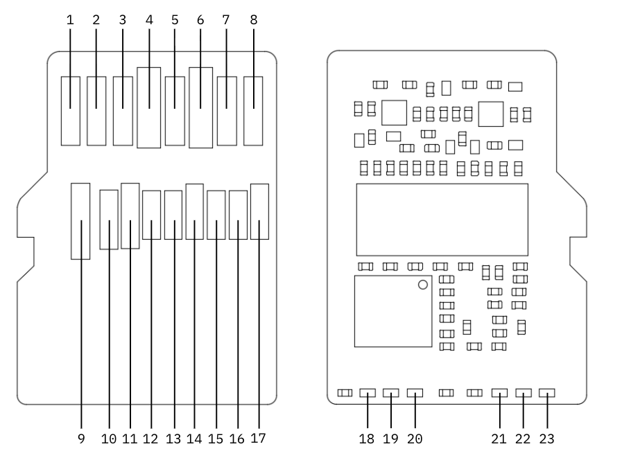
| Pin number | Pin name | Description | Standard |
|---|---|---|---|
| 1 | SD_DAT2 | SD bus DAT2 | LVCMOS 3.3 |
| 2 | SD_DAT3 | SD bus DAT3 | LVCMOS 3.3 |
| 3 | SD_CMD | SD bus CMD | LVCMOS 3.3 |
| 4 | VDD | Supply voltage | |
| 5 | SD_CLK | SD bus CLK | LVCMOS 3.3 |
| 6 | VSS | Supply ground | |
| 7 | SD_DAT0 | SD bus DAT0 | LVCMOS 3.3 |
| 8 | SD_DAT1 | SD bus DAT1 | LVCMOS 3.3 |
| 9 | CONFIG_CSn | SPI configuration port Chip Select | LVCMOS 1.8 |
| 10 | CONFIG_SCLK | SPI configuration port Clock | LVCMOS 1.8 |
| 11 | CONFIG_MOSI | SPI configuration port MOSI | LVCMOS 1.8 |
| 12 | CONFIG_MISO | SPI configuration port MISO | LVCMOS 1.8 |
| 13 | GPIO0 | GPIO pin 0 | LVCMOS 1.8 |
| 14 | N/C | Not connected | |
| 15 | N/C | Not connected | |
| 16 | GPIO1 | GPIO pin 1 | LVCMOS 1.8 |
| 17 | GPIO2 | GPIO pin 2 | LVCMOS 1.8 |
| 18 | RED_LED_0 | Red status LED 0 | |
| 19 | GREEN_LED_0 | Green status LED 0 | |
| 20 | BLUE_LED_0 | Blue status LED 0 | |
| 21 | RED_LED_1 | Red status LED 1 | |
| 22 | GREEN_LED_1 | Green status LED 1 | |
| 23 | BLUE_LED_1 | Blue status LED 1 |
Dimensions and package
The module has overall dimensions of 11 mm × 15 mm × 0.8 mm and fits any standard microSD slot. The drawing below dimensions the outline, with a top view of the board and a side view of the thickness.
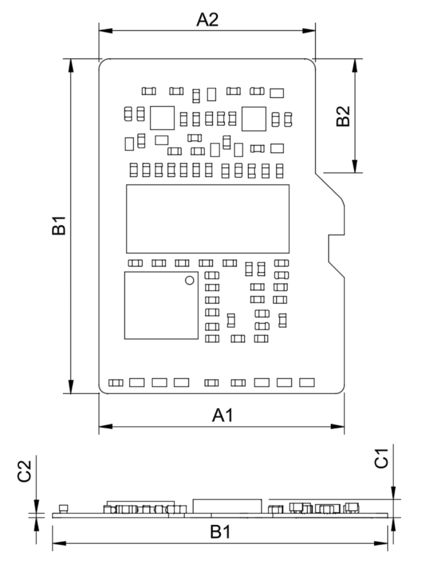
| Dimension | Typical | Tolerance | Unit |
|---|---|---|---|
| A1 | 11 | ± 0.2 | mm |
| A2 | 9.7 | ± 0.2 | mm |
| B1 | 15 | ± 0.2 | mm |
| B2 | 5 | ± 0.2 | mm |
| C1 | 0.8 | ± 0.1 | mm |
| C2 | 0.2 | ± 0.1 | mm |
Next steps
- Design-In Guide, applying these figures to a host board.
- Compatibility, the SD host controllers and platforms tested with the module.
- Benchmarks, measured UxHw speedups against equivalent Monte Carlo workloads.
- Handling and ESD precautions, keeping the module within these conditions in the lab and in the field.