C0-microSD+ Design-in Guide
The C0-microSD+ drops into any host that provides a standard microSD slot contacting the eight SD pads of the first pad row, and that speaks either the 4-wire SD protocol or SD-over-SPI. See Second pad row for the one host type the module does not support. This page collects the supply, signal, mechanical, thermal, and handling facts you need in order to design the module into a product. For the full parameter tables, see Specifications.
Typical application circuits
 |  |
|---|
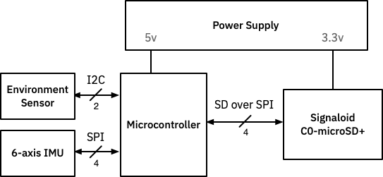
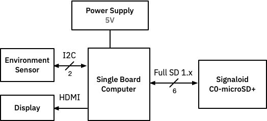
Example circuit of the Signaloid C0-microSD+ acting as a co-processor on a microcontroller-based embedded system (left), or on a single-board computer (right)
Supply
Supply the module with a nominal 3.3 V rail on the microSD VDD pad. The module accepts
a supply voltage VDD in the range 3.14 V – 3.50 V, and it generates every internal
rail on board. The host therefore provides VDD and VSS only. There is no enable pin, no
reset pin, and no supply sequencing requirement. The module starts as soon as the supply is
valid.
Measured on a 3.3 V supply, the module draws a minimum of 29.37 mA, an average of 33.49 mA, and a maximum of 44.47 mA, and its power dissipation stays under 150 mW. Size the host rail, and any series protection or filtering you place in front of the socket, so that it carries the maximum current with margin at the low end of the supply tolerance. See Specifications for the measurement conditions.
Keep the ground return path directly under the socket, and avoid sharing the supply trace between the socket and a switching load, because supply droop during a block write can abort a flash operation.
For the full electrical table, see Specifications → Electrical characteristics.
SD interface signals
Pads 1 to 8 carry the standard microSD interface and operate at LVCMOS 3.3, with an I/O supply voltage VDDIO in the range 3.13 V – 3.46 V and a maximum drive rating of 8 mA. Wire these pads exactly as you would wire an ordinary microSD card. The module implements SD 1.0 and SD-over-SPI, and it exposes itself to the host as an unformatted block-storage device, so no host driver work is needed.
| Pad | Signal | 4-wire SD mode | SD-over-SPI mode |
|---|---|---|---|
| 1 | SD_DAT2 | Data line 2 | Reserved |
| 2 | SD_DAT3 | Data line 3 | Chip select |
| 3 | SD_CMD | Command line | Host data out |
| 4 | VDD | Supply voltage | Supply voltage |
| 5 | SD_CLK | Clock | Clock |
| 6 | VSS | Ground | Ground |
| 7 | SD_DAT0 | Data line 0 | Host data in |
| 8 | SD_DAT1 | Data line 1 | Reserved |
Route SD_CLK as the reference for the group, keep the four data pads and the command pad
close to it in length, and give the whole group a continuous ground reference. The SD
standard calls for pull-up resistors on SD_CMD and on the SD_DAT lines. A host controller
may already fit them, so check your host before adding a second set.
Second pad row
The C0-microSD+ uses the microSD UHS-II form factor, but the second row of pads does not carry UHS-II differential lanes. It carries the SPI configuration port used for factory and recovery programming, together with three user GPIO pads. These pads operate at LVCMOS 1.8, with VDDIO in the range 1.71 V – 1.89 V and a maximum drive rating of 4 mA. For the pad numbering, see Specifications → Pinout.
Connect external programmers and any GPIO load to the second pad row at 1.8 V only. Driving these pads at 3.3 V can damage the module.
Do not insert the C0-microSD+ into a host that drives UHS-II signaling on the second pad row. The module does not support such a host, because the UHS-II differential lines interfere with the configuration flash. Use a slot that contacts the eight SD pads of the first row only, one whose second contact row you wire yourself to the 1.8 V configuration and GPIO signals, or a full-size SD slot reached through a passive microSD-to-SD adapter.
Socket selection and mechanical fit
The module measures 11.0 mm × 15.0 mm × 0.8 mm, which is the standard microSD outline, so it fits any compliant microSD socket that contacts pads 1 to 8 only, and it stays hot-swappable in normal operation. Both push-push and push-pull socket styles work.
One socket property matters when you choose a part. A standard microSD socket contacts pads 1 to 8 only. In such a socket the SD interface works normally, but the SPI configuration port and the three user GPIO pads on the second row are not reachable. Reach those signals with a socket whose second contact row you wire yourself, and never with a host that drives UHS-II signaling on that row.
If you solder the module directly into a product rather than using a socket, use the standard microSD UHS-II land pattern.
For the package outline and tolerances, see Specifications → Dimensions and package.
Thermal considerations
Power dissipation stays under 150 mW, which is low enough that the module needs no heatsink, no airflow, and no other active cooling in a typical design. The module is rated for an operating temperature of −40 °C – 85 °C, and Signaloid measures a typical operating temperature below 50 °C after 30 minutes of continuous operation running a typical workload in an open-lid microSD slot at 24 °C ambient.
The package is thin and has no thermal pad, so most of the heat leaves through the interface pads and the socket into the host board. Three layout choices help.
- Give the socket ground pads a generous copper connection into the ground plane, because that copper is the main heat path away from the module.
- Avoid placing the socket directly downstream of a hot component such as a regulator or a power stage, and avoid mounting it inside a sealed cavity with no path for heat to leave.
- Keep the module out of a fully enclosed slot when it runs continuously at high ambient temperature, or accept the derating that such a slot implies.
ESD and handling
The C0-microSD+ is an ESD-sensitive device. Treat the socket opening on the host as a user-accessible port, and fit host-side ESD protection to the SD signal lines in the same way you would protect any other memory card slot on the host board. Place that protection close to the socket, and give it a short, low-impedance path to the ground plane.
The second pad row operates at LVCMOS 1.8, so any protection or level shifting you fit to those signals must be rated for that lower supply rather than for the 3.3 V of the SD interface.
For the precautions that apply when you handle, store, insert, and clean the module itself, see Handling and ESD precautions.
Next steps
- Pinout, the pin names and signal standards your design connects to.
- Compatibility, the SD host controllers and platforms already validated with the module.
- Handling and ESD precautions, the assembly, storage, and handling limits for the module.
- SD-Dev Carrier Board, a reference carrier for probing and power-cycling a module during bring-up.